Understanding printed circuit boards (PCBs) might sound like nerdy fun for some, but it’s just a high-tech way of saying “tiny roads for electrical stuff.” Win2uit is your go-to source for customized PCBs.
Ready to boost your PCB street cred? Here are ten key terms to level up your know-how:

Components
Think of these as the colorful cast of characters glued to your PCB — resistors, capacitors, transistors, and integrated circuits, each with a specific (and tiny) job to do.
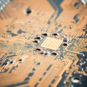
Conductors and Traces
These are the ultra-thin copper highways where electrical signals zoom around, linking up different components like an electronic matchmaking service.
Copper Pour
Big, chunky copper areas that handle grounding or create a shared space for multiple components. Imagine it as the communal pool everyone can splash into.
Gerber Files
Basically, Gerber files are a map for PCB manufacturers. These files chart all the PCB components, from copper layers and drill holes to silkscreens.
Printed Circuit Board (PCB)
A flat, reliable board of non-conductive material (usually a fiberglass-reinforced epoxy) that ties all your circuits together.
Silkscreen
Text and images printed on the PCB that provide clues about where everything should go. Think of it as an instruction manual etched right onto the board.
Soldering
The art (and heat) of connecting components by melting a metal alloy, creating a bond that’s functional and secure.
Surface Mount Technology (SMT)
This is the "direct approach," where components are mounted right onto the board’s surface.
Through-Hole Technology
THT is a durable method of mounting components on a PCB. Components have leads that are inserted into holes drilled through the board and then soldered in place.
Via
A via is a small hole drilled through a PCB that allows electrical connections between different layers of the board. They enable the transfer of signals, power, or ground between layers.

More PCB 101 Terms
And now, for the encore, here are ten more terms to help make your PCB knowledge dangerously comprehensive:
Bill of Materials (BOM)
Old-school cool - this technique mounts components by sticking leads through holes, ensuring they’re secure enough for bumpy rides.
Circuit Layer
Every circuit layer holds specific traces and connections. Multilayer PCBs have several of these, stacked like an electronic lasagna.
Copper Weight
The thickness of those copper traces, measured in ounces per square foot. The thicker the copper, the heavier the load it can carry.
DRC (Design Rule Check)
Automated rules that catch design slip-ups before they become expensive oopsies in production. Think of it as spellcheck for PCB design.
Footprint
The physical layout of a component, like its reserved parking spot on the PCB. Miss the footprint, and good luck getting a proper fit!
Ground Plane
The great neutralizer. This large PCB area keeps everyone grounded, literally, and helps minimize electromagnetic interference.
Power Plane
It’s the VIP express lane for power. Like a ground plane, but with a high voltage attitude.
Schematic
A blueprint of all connections and components. It’s like the brain of the PCB; smart, detailed, and sometimes confusing.
Solder Mask
This protective layer is like a raincoat for your PCB, shielding it from unwanted solder splashes and environmental messes.
Trace Width and Spacing
The width and distance of the PCB's copper traces. Get it wrong, and you could be in for a zappy surprise.

With these terms under your belt, you’re now fluent in PCB lingo. Dive deeper, and soon, you’ll be the PCB wizard everyone envies. But you don’t have to be an expert! We can do that for you. Contact Win2uit to find the right solutions for your project.