When you begin the journey of efficient PCB layout design, you’ll quickly realize it’s more than dropping parts and drawing traces. It’s about balancing performance, manufacturability, and reliability so your board actually works in the real world. Here are advanced strategies to help you design smarter and avoid costly surprises.

Component Placement
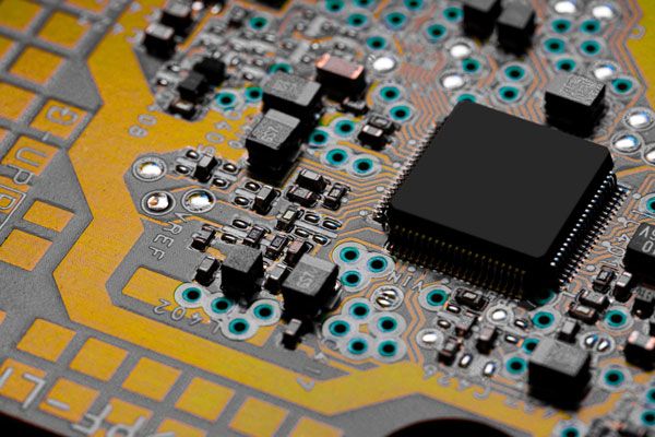
When placing components on your PCB, start with the most critical elements, such as the microcontroller or power supply. Locking in these anchors first helps guarantee proper spacing and optimal performance across the board.
Next, group components by function. Clustering related parts reduces signal paths and lowers the risk of interference. For example, keep analog circuitry separated from digital sections to avoid noise issues.
High-speed components should live close to their connectors to minimize trace length and preserve signal integrity.

Thermal planning matters, too. Position heat-generating components, such as voltage regulators and power transistors, away from sensitive devices. Leave room for heat sinks or airflow where needed, and place decoupling capacitors close to power pins to stabilize voltage and filter noise.
Don’t overlook manufacturability. Align components to simplify soldering and inspection and maintain consistent orientation for polarized parts to reduce assembly errors.
Finally, respect mechanical constraints. Maintain proper clearances around mounting holes, connectors, and enclosure boundaries to avoid expensive redesigns later.
Signal Routing Techniques
With components in place, routing becomes the next big lever for performance.

Keep traces short and direct whenever possible. This reduces resistance and inductance, improves signal speed, and minimizes noise pickup.
Avoid sharp 90-degree trace angles. Use 45-degree routing to maintain signal integrity and reduce reflections.
Separate high-speed signals from low-speed lines to prevent interference. Differential pairs should be routed tightly together to maintain impedance control and minimize EMI. Sensitive analog traces should be kept far from noisy digital routing to prevent crosstalk.
Use vias thoughtfully. Excessive vias introduce parasitic inductance and capacitance that can degrade signal quality. When vias are necessary, place them carefully and keep signal paths as continuous as possible.
Proper termination also matters. Series or parallel termination resistors help match impedance and reduce reflections on fast edges.
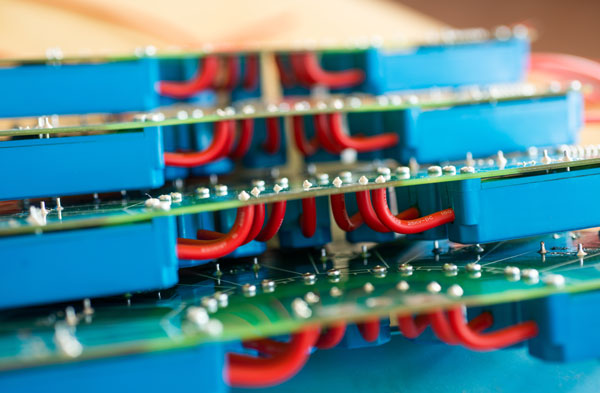
Power and Ground Planes
Well-designed power and ground planes are the backbone of a stable PCB.
Whenever possible, dedicate solid layers to power and ground and keep them continuous. Unbroken planes help prevent voltage drops and reduce EMI.

Maximize copper usage for these planes. More copper means lower resistance and better thermal performance. Place the power plane adjacent to the ground plane to create a low-inductance path that supports high-speed signal integrity.
Avoid splitting the ground plane unless absolutely necessary. Splits can create return-path problems and introduce noise.
During routing, ensure signal return paths flow cleanly over the ground plane to minimize loop area. Use multiple vias to connect planes and evenly distribute current, lowering overall impedance.
Place decoupling capacitors close to IC power pins, bridging power and ground to filter noise effectively.
Thermal Management
Even the cleanest electrical design can fail if heat isn’t managed properly.
Start by spacing out high-power components, so heat can dissipate naturally. Avoid clustering hot parts in one area. Use thermal vias to move heat from hot spots to cooler board layers. Tie these vias into large copper pours that act as heat spreaders.
For higher power designs, consider heat sinks or thermal pads directly on components. Thicker copper weights can also improve heat flow by lowering thermal resistance. If the PCB will live inside an enclosure, plan for airflow. Strategic venting or fan placement can dramatically improve both passive and active cooling performance.
Design for Manufacturability
A brilliant design that’s hard to build is still a problem. Design for manufacturability (DFM) from the start.
Standardize component sizes and packages where possible. Using common, readily available parts helps avoid supply chain headaches and simplifies assembly. Maintain consistent component spacing to support automated pick-and-place processes. Crowded or misaligned parts often lead to manual rework and higher costs.
Size vias and traces appropriately and avoid unnecessary complexity. Simpler layouts generally yield higher manufacturing yields. Also, consider the layer count carefully. Each additional layer increases cost and fabrication complexity, so only add layers when they deliver real value.
Most importantly, collaborate early with your manufacturing partner. The sooner manufacturability is reviewed, the fewer surprises you’ll face later.
Why Early DFM Review Matters
Modern design workflows move fast, but skipping early manufacturability checks can slow everything down later.
Running a DFM review early helps you:
- Catch spacing and clearance issues.
- Identify potential yield problems.
- Reduce costly respins
- Shorten the time to production.
Many teams build this review step directly into their release process to keep projects on track and production ready.
Testing and Validation
Once your layout is manufacturable, rigorous testing is the final gate before production.
Build and evaluate a prototype under real-world conditions. Verify electrical performance, thermal behavior, and mechanical fit. Look for signal integrity issues, power stability, and any unexpected heat buildup. Environmental and stress testing can also reveal weaknesses that don’t show up on the bench.
If you need support evaluating your design or selecting the right production partner, the team at Win2uit can help guide next steps and connect you with the right resources.
Strong PCB layout design isn’t about luck. It’s about disciplined placement, clean routing, solid planes, smart thermal planning, and building manufacturability into the process from day one. Nail those fundamentals, and your boards will perform exactly the way you intended.