Let’s keep this simple.
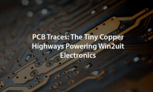
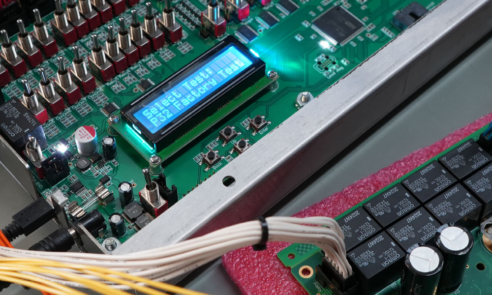
Inside every control board is a printed circuit board (PCB). And running across that board are thin copper lines called traces. Think of them like tiny highways that move electricity from point A to point B.
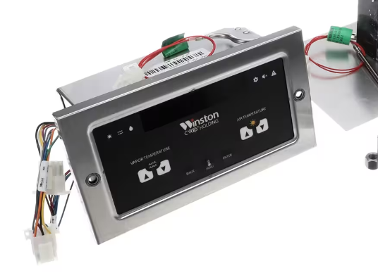
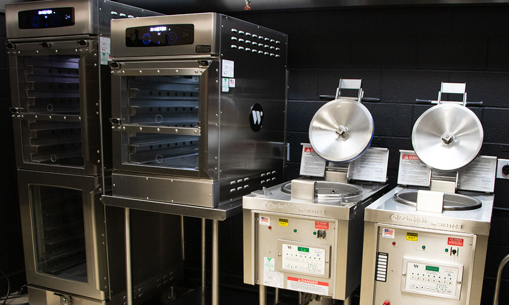
At Winston, those little copper paths have a big job. All of the electronics for Winston CVap equipment and Collectramatic Fryers are built at Win2uit. They have to perform consistently in real kitchens — heat, humidity, long days, zero patience for failure.
Here’s what PCB traces are doing behind the scenes:
- Carry electrical signals
- Deliver power to components.
- Help keep timing and signal quality clean.
- Move heat away from sensitive parts.
You don’t have to be an engineer to understand this: when traces are well-designed and built, equipment runs smoother and lasts longer. When they’re not… problems show up fast.
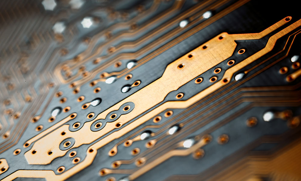
Copper: Where Every Trace Begins
Every trace starts as a sheet of copper bonded to the circuit board.
Why copper? Because it checks all the right boxes:
- Excellent electrical conductor
- Easy to manufacture
- Reliable overtime
- Cost-effective
Copper thickness is measured in ounces per square foot. In plain English: thicker copper can carry more electrical current and handle more heat.
This matters to boards that have to operate in harsh environments, such as commercial kitchens. Components get warm. Equipment runs hard. We design for real-world conditions, not lab fantasies.
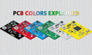
Not All Copper Is Created Equal
Here’s where things get interesting.
PCB manufacturers don’t just grab any copper and call it a day. The type and quality of copper foil directly affect how well those traces perform.
Better copper means:
- Cleaner signal flow
- More reliable current handling
- Better durability during heating and cooling cycles
To create traces, manufacturers etch away the copper they don’t need, leaving behind the precise pathways the design calls for.
The smoother and more uniform the starting copper is, the cleaner the finished trace will be.
For example:
- Rolled-annealed copper is more flexible and less prone to cracking.
- Ultra-smooth copper supports very fine, tightly packed trace designs.
Translation: smart material choices up front prevent headaches later.
Fast-Turn Assembly: Moving Fast Without Cutting Corners
In product development, speed matters. But let’s be clear, fast only works if it’s also accurate.
Modern PCB partners can deliver fast-turn prototype boards in as little as 24 to 72 hours. That’s impressive. But it only works when the trace geometry is tightly controlled and repeatable.
When traces are clean and consistent:
- Builds move faster
- Rework drops
- Prototypes behave the way engineers expect
Well-formed traces also help prevent common assembly issues like:
- Solder bridges
- Components standing up (“tombstoning”)
- Poor solder flow
In other words, good traces make life easier for everyone downstream.
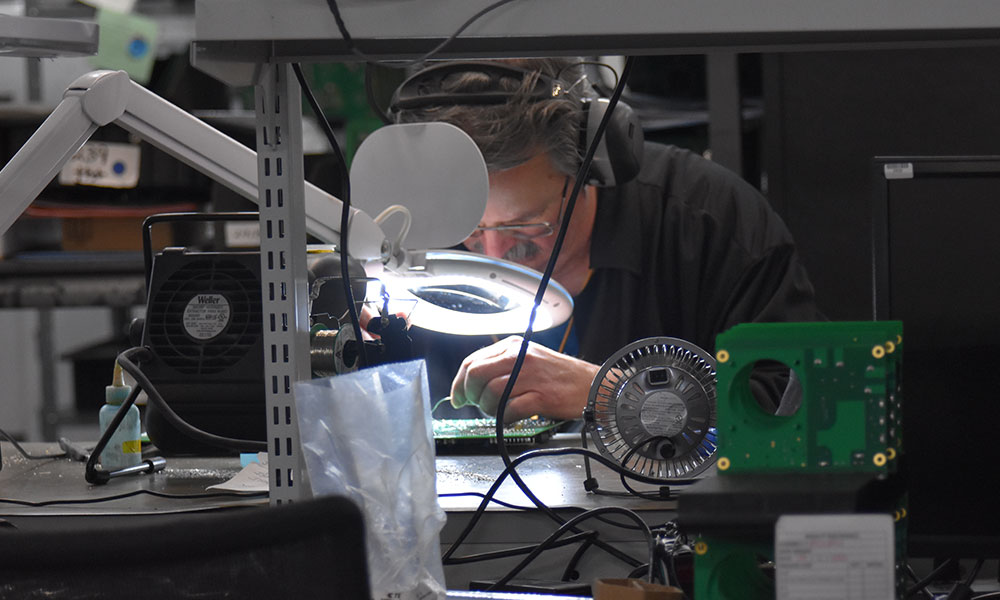
Testing: Because “Looks Good” Isn’t Good Enough
At Winston, reliability isn’t optional. So quality PCB manufacturers don’t just build boards and hope for the best. They test. Then they test again.
Typical quality checks include:
- Automated Optical Inspection (AOI)
- Electrical testing with flying probes or bed-of-nails fixtures
- Cross-sectional analysis of the board
- X-ray inspection
- Impedance measurement
All of this work confirms the things that really matter:
- Trace widths are correct.
- Plating thickness meets spec.
- Vias are solid and void-free.
- Board layers are uniform.
It’s a lot of behind-the-scenes work that leads to one simple outcome: boards you can trust.
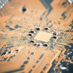
Microvias: Tiny Upgrade, Big Payoff
Let’s talk about one of the quieter improvements in modern PCB design.
A via is a small plated hole that connects one layer of the board to another. Traditional vias have worked for years, but they take up space and can slightly distort high-speed signals.
Newer designs often use microvias, which are:
- Laser-drilled
- Much smaller
- Much shorter
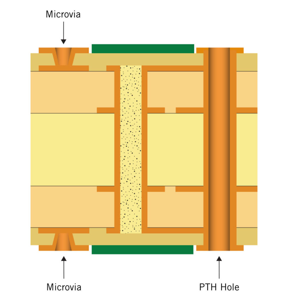
Because they’re so compact, microvias:
- Improve signal clarity
- Reduce electrical noise
- Free up routing space on dense boards
- Support higher-performance electronics
A via is a tiny plated hole that connects different layers of a circuit board. It allows electricity to move vertically through the board, which is essential in modern multilayer designs.
Fast-turn assembly is rapid PCB prototyping that usually delivers small batches in 24 to 72 hours. It helps engineers test and refine designs quickly.
Traces are the copper paths that connect components on a circuit board. Their width and spacing determine how safely they carry power and how cleanly signals travel.
PCB traces may be small, but they do heavy lifting inside Win2uit electronics. When the copper is right, the design is tight, and the manufacturing is controlled, everything downstream gets better:
- Cleaner signals
- More reliable performance
- Faster, smoother assembly
- Fewer surprises in the field
At Win2uit, that’s the goal every time. Because in real electronics, you don’t get points for trying. It has to work. Every shift. Every day.